- 您现在的位置:买卖IC网 > Sheet目录2000 > IDT23S08-1HPGI8 (IDT, Integrated Device Technology Inc)IC CLK MULT PLL HI DRV 16-TSSOP
4
COMMERCIALANDINDUSTRIALTEMPERATURERANGES
IDT23S08
3.3V ZERO DELAY CLOCK MULTIPLIER
ZERO DELAY AND SKEW CONTROL
To close the feedback loop of the IDT23S08, the FBK pin can be driven from any of the eight available output pins. The output driving the FBK pin
will be driving a total load of 7pF plus any additional load that it drives. The relative loading of this output (with respect to the remaining outputs) can adjust
the input-output delay.
For applications requiring zero input-output delay, all outputs including the one providing feedback should be equally loaded. Ensure the outputs are
loaded equally, for zero output-output skew.
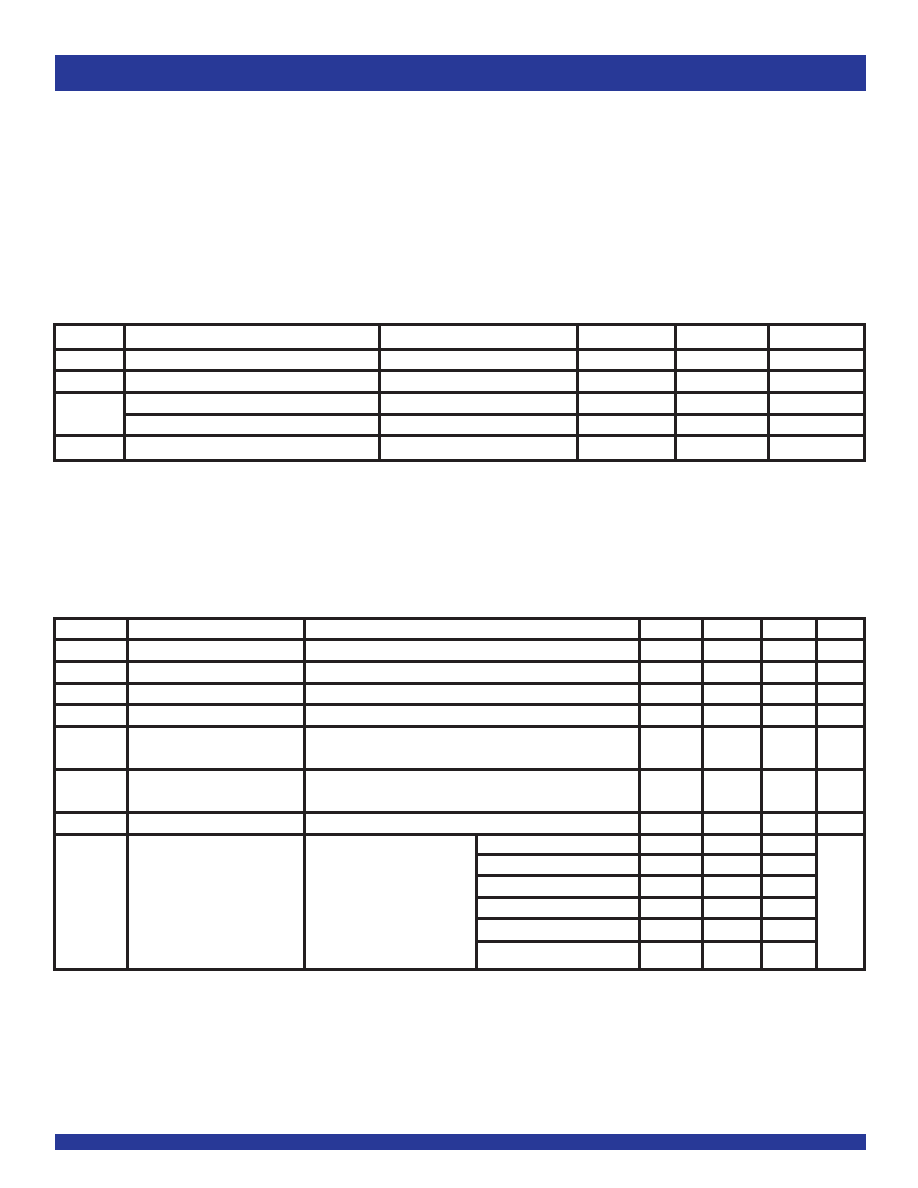
DC ELECTRICAL CHARACTERISTICS - COMMERCIAL
Symbol
Parameter
Conditions
Min.
Typ.(1)
Max.
Unit
VIL
InputLOWVoltageLevel
—
0.8
V
VIH
Input HIGH Voltage Level
2
—
V
IIL
InputLOWCurrent
VIN = 0V
—
50
A
IIH
Input HIGH Current
VIN = VDD
—
100
A
VOL
OutputLOWVoltage
IOL = 8mA (-1, -2, -3, -4)
—
0.4
V
IOL = 12mA (-1H, -2H, -5H)
VOH
Output HIGH Voltage
IOH = -8mA (-1, -2, -3, -4)
2.4
—
V
IOH = -12mA (-1H, -2H, -5H)
IDD_PD
Power Down Current
REF = 0MHz (S2 = S1 = H)
—
12
A
100MHz CLKA (-1, -2, -3, -4)
—
45
100MHz CLKA (-1H, -2H, -5H)
—
70
IDD
SupplyCurrent
UnloadedOutputs
66MHz CLKA (-1, -2, -3, -4)
—
32
mA
Select Inputs at VDD or GND
66MHz CLKA (-1H, -2H, -5H)
—
50
33MHz CLKA (-1, -2, -3, -4)
—
18
33MHz CLKA (-1H, -2H, -5H)
—
30
NOTE:
1. Applies to both REF and FBK.
Symbol
Parameter
Test Conditions
Min.
Max.
Unit
VDD
SupplyVoltage
3
3.6
V
TA
OperatingTemperature(AmbientTemperature)
0
70
°C
CL
Load Capacitance below 100MHz
—
30
pF
Load Capacitance from 100MHz to 133MHz
—
15
pF
CIN
InputCapacitance(1)
—7
pF
OPERATING CONDITIONS- COMMERCIAL
发布紧急采购,3分钟左右您将得到回复。
相关PDF资料
IDT23S08T-1DC
IC CLK MULT PLL ZD 2.5V 16-SOIC
IDT23S09T-1DC8
IC CLK BUFFER ZD 2.5V 16-SOIC
IDT5T929-30NLGI
IC CLOCK GENERATOR PREC 28VFQFPN
IDT5T940-10NLGI
IC CLK GENERATOR PREC 28-VFQFPN
IDT5T9820NLI8
IC CLK DRIVER ZD PLL 68-VFQFPN
IDT5T9890NLI8
IC CLK DRIVER 2.5V PLL 68-VFQFPN
IDT5V19EE604NDGI8
IC PLL CLK GEN 200MHZ 28VFQFPN
IDT5V40501DVG
IC CLK GEN PLL 160MHZ 8TSSOP
相关代理商/技术参数
IDT23S08-2
制造商:IDT 制造商全称:Integrated Device Technology 功能描述:3.3V ZERO DELAY CLOCK MULTIPLIER, SPREAD SPECTRUM COMPATIBLE
IDT23S08-2DC
功能描述:IC CLK MULT PLL STD DRV 16-SOIC RoHS:否 类别:集成电路 (IC) >> 时钟/计时 - 时钟发生器,PLL,频率合成器 系列:- 产品变化通告:Product Discontinuation 04/May/2011 标准包装:96 系列:- 类型:时钟倍频器,零延迟缓冲器 PLL:带旁路 输入:LVTTL 输出:LVTTL 电路数:1 比率 - 输入:输出:1:8 差分 - 输入:输出:无/无 频率 - 最大:133.3MHz 除法器/乘法器:是/无 电源电压:3 V ~ 3.6 V 工作温度:0°C ~ 70°C 安装类型:表面贴装 封装/外壳:16-TSSOP(0.173",4.40mm 宽) 供应商设备封装:16-TSSOP 包装:管件 其它名称:23S08-5HPGG
IDT23S08-2DC8
功能描述:IC CLK MULT PLL STD DRV 16-SOIC RoHS:否 类别:集成电路 (IC) >> 时钟/计时 - 时钟发生器,PLL,频率合成器 系列:- 产品变化通告:Product Discontinuation 04/May/2011 标准包装:96 系列:- 类型:时钟倍频器,零延迟缓冲器 PLL:带旁路 输入:LVTTL 输出:LVTTL 电路数:1 比率 - 输入:输出:1:8 差分 - 输入:输出:无/无 频率 - 最大:133.3MHz 除法器/乘法器:是/无 电源电压:3 V ~ 3.6 V 工作温度:0°C ~ 70°C 安装类型:表面贴装 封装/外壳:16-TSSOP(0.173",4.40mm 宽) 供应商设备封装:16-TSSOP 包装:管件 其它名称:23S08-5HPGG
IDT23S08-2DCG
功能描述:IC CLK MULT PLL STD DRV 16-SOIC RoHS:是 类别:集成电路 (IC) >> 时钟/计时 - 时钟发生器,PLL,频率合成器 系列:- 标准包装:2,000 系列:- 类型:PLL 时钟发生器 PLL:带旁路 输入:LVCMOS,LVPECL 输出:LVCMOS 电路数:1 比率 - 输入:输出:2:11 差分 - 输入:输出:是/无 频率 - 最大:240MHz 除法器/乘法器:是/无 电源电压:3.135 V ~ 3.465 V 工作温度:0°C ~ 70°C 安装类型:表面贴装 封装/外壳:32-LQFP 供应商设备封装:32-TQFP(7x7) 包装:带卷 (TR)
IDT23S08-2DCG8
功能描述:IC CLK MULT PLL STD DRV 16-SOIC RoHS:是 类别:集成电路 (IC) >> 时钟/计时 - 时钟发生器,PLL,频率合成器 系列:- 标准包装:2,000 系列:- 类型:PLL 时钟发生器 PLL:带旁路 输入:LVCMOS,LVPECL 输出:LVCMOS 电路数:1 比率 - 输入:输出:2:11 差分 - 输入:输出:是/无 频率 - 最大:240MHz 除法器/乘法器:是/无 电源电压:3.135 V ~ 3.465 V 工作温度:0°C ~ 70°C 安装类型:表面贴装 封装/外壳:32-LQFP 供应商设备封装:32-TQFP(7x7) 包装:带卷 (TR)
IDT23S08-2DCGI
功能描述:IC CLK MULT PLL STD DRV 16-SOIC RoHS:是 类别:集成电路 (IC) >> 时钟/计时 - 时钟发生器,PLL,频率合成器 系列:- 标准包装:2,000 系列:- 类型:PLL 时钟发生器 PLL:带旁路 输入:LVCMOS,LVPECL 输出:LVCMOS 电路数:1 比率 - 输入:输出:2:11 差分 - 输入:输出:是/无 频率 - 最大:240MHz 除法器/乘法器:是/无 电源电压:3.135 V ~ 3.465 V 工作温度:0°C ~ 70°C 安装类型:表面贴装 封装/外壳:32-LQFP 供应商设备封装:32-TQFP(7x7) 包装:带卷 (TR)
IDT23S08-2DCGI8
功能描述:IC CLK MULT PLL STD DRV 16-SOIC RoHS:是 类别:集成电路 (IC) >> 时钟/计时 - 时钟发生器,PLL,频率合成器 系列:- 标准包装:2,000 系列:- 类型:PLL 时钟发生器 PLL:带旁路 输入:LVCMOS,LVPECL 输出:LVCMOS 电路数:1 比率 - 输入:输出:2:11 差分 - 输入:输出:是/无 频率 - 最大:240MHz 除法器/乘法器:是/无 电源电压:3.135 V ~ 3.465 V 工作温度:0°C ~ 70°C 安装类型:表面贴装 封装/外壳:32-LQFP 供应商设备封装:32-TQFP(7x7) 包装:带卷 (TR)
IDT23S08-2DCI
功能描述:IC CLK MULT PLL STD DRV 16-SOIC RoHS:否 类别:集成电路 (IC) >> 时钟/计时 - 时钟发生器,PLL,频率合成器 系列:- 产品变化通告:Product Discontinuation 04/May/2011 标准包装:96 系列:- 类型:时钟倍频器,零延迟缓冲器 PLL:带旁路 输入:LVTTL 输出:LVTTL 电路数:1 比率 - 输入:输出:1:8 差分 - 输入:输出:无/无 频率 - 最大:133.3MHz 除法器/乘法器:是/无 电源电压:3 V ~ 3.6 V 工作温度:0°C ~ 70°C 安装类型:表面贴装 封装/外壳:16-TSSOP(0.173",4.40mm 宽) 供应商设备封装:16-TSSOP 包装:管件 其它名称:23S08-5HPGG